
Common FPGA interview questions
 I compiled some of the common FPGA interview questions I encountered over the years while seeking digital design positions:
1. FIFO depth calculation
How do you calculate the depth of the FIFO you need?
Fifo depth calculation:
Write clk freq – Fw
Read clk freq – Fr
Writing burst size: B
Idle clk cycle # for reading side – I
Fifo depth = B – B * Fr/(Fw*I)
Another approach (example with actual numbers):
Burst of 200 bytes
Fw=100mhz, Fr=50mhz
One byte read & one byte written each cycle
Time to write 1 byte: 1/100=10ns
Time to write 200 bytes=2000ns
Time to read 1 byte: 1/50=20ns
The number of bytes read while writing= 2000ns/20ns=100
Fifo depth=200-100=100 bytes
2. Metastability
What is metastability?
Definition from wikipedia:
Metastability in electronics is the ability of a digital electronic system to persist for an unbounded time in an unstable equilibrium or metastable state. In metastable states, the circuit may be unable to settle into a stable ‘0’ or ‘1’ logic level within the time required for proper circuit operation. As a result, the circuit can act in unpredictable ways, and may lead to a system failure, sometimes referred to as a “glitch”.
Metastable states are inherent features of asynchronous digital systems, and of systems with more than one independent clock domain. In self-timed asynchronous systems, arbiters are designed to allow the system to proceed only after the metastability has resolved, so the metastability is a normal condition, not an error condition. In synchronous systems with asynchronous inputs, synchronizers are designed to make the probability of a synchronization failure acceptably small. Metastable states are avoidable in fully synchronous systems when the input setup and hold timerequirements on flip-flops are satisfied.
3. Setup and Hold time equations
Setup time formula
Tc2q + Tcomb + Tsetup <= Tclk + Tskew Hold time formula Tc2q + Tcomb >= Thold + Tskew
Tc2q: Delay from the clock edge to the output of the flip flop
Tcomb: Combinatorial delay
Tsetup: Setup time of the FF (flip flop)
Tclk: Clock period
Tskew: Clock skew
Thold: Hold time of the FF
Actually, instead of Tcomb, Tprop (propagation delay) may have been a more accurate representation of the delay in question, since it would include both the logic delay, and also the routing delay for the signal. But the combinatorial delay is the important part of this delay, and it is the one commonly used in these equations.
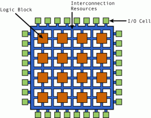
4. What is a CLB?
CLB refers to the “Configurable Logic Block”s in Xilinx FPGAs
Spartan3 CLB:
4 Slices, each slice has 2 LUTs, 2 FFs
LUTs have 4 inputs
Spartan6 CLB:
2 Slices, each slice has 4 LUTs, 8 FFs
LUTs have 6 inputs. These basic slices are called SliceX. Some slices also have multipliers and carry logic, and they are called SliceLs. And some slices also have capability to use LUTs as distributed RAMs, and also as variable length shift registers. They are called SliceMs.
Virtex6 CLB:
Same as Spartan6. But basic slices are SliceLs. And it also has SliceMs.
7 Series CLB:
LUTs can be configured as 1 6-input LUT, or 2 5-input LUTs. Each slice has 4 6-input LUTs, and 8 FFs. Each CLB has 2 slices. 2/3 of slices are SliceLs, others are SliceMs.
Ultrascale CLB:
Each CLB has one slice, but 2 slices of the 7 series is combined into one cohesive slice. So, each slice has 8 LUTs, and 16 FFs.
Altera has ALM instead of CLB
ALM: Adaptive Logic Module
It has 8 inputs for its LUT, which can implement a full 6-input LUT, or 7 input functions. Each ALM has one of these LUTs, and 2 FFs.
5. Clock management blocks in FPGAs
In Xilinx FPGAs:
Older families like Spartan 3 had DCMs (digital clock manager). New families have CMTs (clock management tile). CMTs have MMCMs and PLLs in them.
6. What are the transceiver types and speeds in Xilinx FPGAs?
Transceivers:
GTP: 6 gbps
GTX: 12.5 gbps
GTH: 13.1 gbps
GTY: 28 gbps on ultrascale, 32 gbps on ultrascale +
UltraScale+ GTR (6.0 Gb/s): Easiest integration of common protocols to the Zynq Processor Subsystem
UltraScale+ GTH (16.3 Gb/s): Low power & high performance for the toughest backplanes
UltraScale+ GTY (32.75 Gb/s): Maximum performance for the fastest optical and backplane applications; 33G transceivers for chip-to-chip, chip-to-optics, and 28G backplanes
UltraScale GTH (16.3 Gb/s): Low power & high performance for the toughest backplanes
UltraScale GTY (30.5 Gb/s): High performance for optical and backplane applications; 30G transceivers for chip-to-chip, chip-to-optics, and 28G backplanes
7 Series GTP (6.6 Gb/s): Power optimized transceiver for consumer and legacy serial standards
7 Series GTX (12.5 Gb/s): Lowest jitter and strongest equalization in a mid-range transceiver
7 Series GTH (13.1 Gb/s): Backplane and optical performance through world class jitter and equalization
7 Series GTZ (28.05 Gb/s): Highest rate, lowest jitter 28G transceiver in a 28nm FPGA